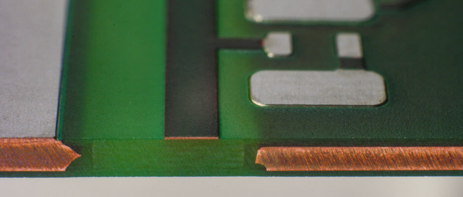
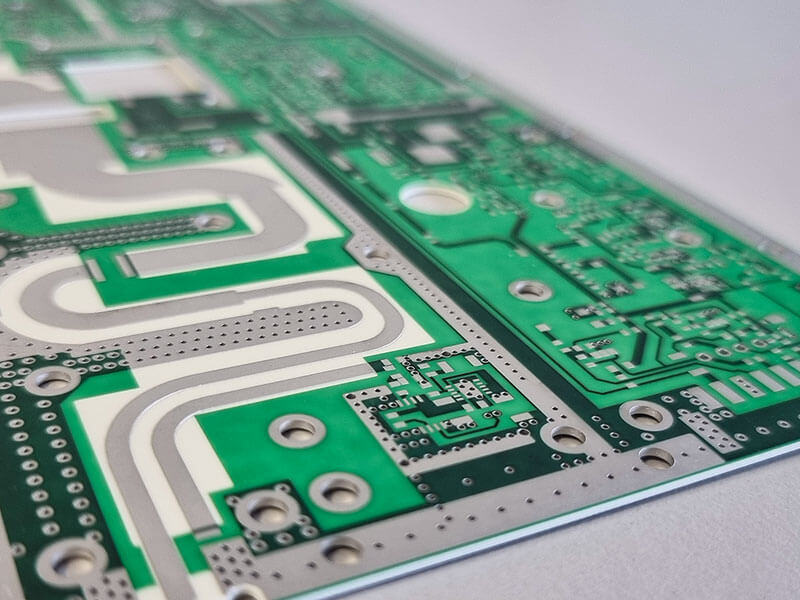
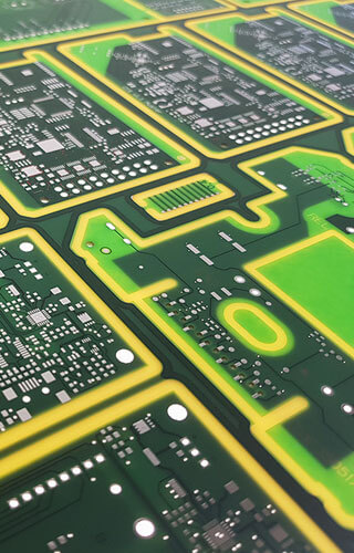
The accommodation of power electronics and the associated extremely high current intensities require special specifications of the carrier circuit boards. The focus is on the profile of the copper traces – copper layers of up to 1,000 μm on inner/outer layers enable an optimal flow of current while keeping the trace heating limited. At Becker & Müller we use copper foils in thicknesses of 105/200/400/1,000 μm for the production of high-current and thick-copper PCB. Further thicknesses and special inlays with inlaid copper parts are also on request available.
For what are high-current and thick-copper PCB needed?
Application areas of high-current and thick-copper PCB are everywhere where high currents or a special heat management are required. Current examples, in additions to general power supply, are also drive technology – keyword e-mobility – as well as converters for solar and wind power plants.
In order to meet these (new) technical requirements, thermal management, reduction of size and assembly costs are required. Even the intention to integrate control and power sections together on one circuit board pose challenges for developers, layouters and PCB manufacturers – see here also our copper-inlay-technology below.
In manufacturing of high-current and thick-copper PCB a special challenging part is to ensure the uniformity of the etched trace layout as well as the fully covering application of the solder mask. Here there are special design rules such as trace width/distance etc. to observe. By years of experience as well as a high process reliability in production at Becker & Müller these requirements are implemented with absolute reliability. In order to be able to use all the possibilities of this technology optimally, a coordination between developer, layouter and PCB manufacturer is decisive. We at Becker & Müller will be happy to be available to our customers personally as a development partner for individual advices.
As an experienced manufacturer of high-current and thick-copper PCB Becker & Müller is very familiar with the specific advantages. These include in particular:
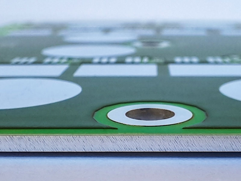
direct heat dissipation -> Components can be fitted and soldered directly with a copper core that protrudes from the FR4 insulation at crucial points
copper layers on the remaining areas of the PCB can be selected as desired -> fine pitch elements can be used
saving of space (by integration of control and power unit)
simplification of assembly and cost reduction (by saving of fasteners)
In demanding performance areas such as high-current and thick-copper circuit boards especially the coordination between developer, layout and PCB manufacturer is indispensable. We at Becker & Müller as an experienced professional in PCB manufacturing are happy to be available to customers for individual advices – either via phone or directly at the customer’s.
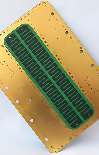
Copper-inlay-technology
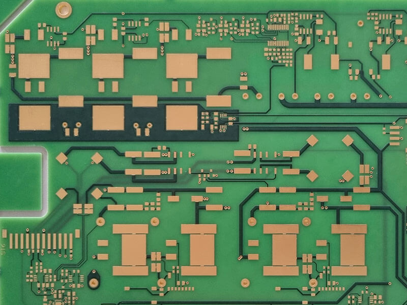
The use of copper-inlay-technology enables to integrate the power and control part on a single circuit board without mutual influence. The power section requires large and coarse structures to transport the extremely high currents respectively to be able to optimally dissipate the heat development. The control section on the other hand needs fine structures on which there is a lower current flow. The challenge is to combine both sections on a single circuit board. Here we at Becker & Müller are experienced specialists.
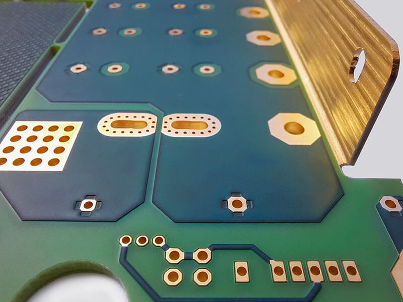
The copper-inlay-technology offers a method with which copper inlay cores with a thickness of up to 4 mm – standard inlays measure 1 mm – can be inserted in a multilayer or directly applied on the surface of the PCB. To make optimal use of the possibilities of this technology a coordination between developer, layouter and PCB manufacturer is crucial. That is why we at Becker & Müller are already at the DFM process (Design For Manufacturing) personally available.
Advantages of copper-inlay-technology:
copper inlay core up to 4 mm thickness
direct heat dissipation -> copper core that protrudes from FR4 at critical points, directly fitted and soldered with components
saving of space
reducing costs (by saving of material and components)
current strength up to 1,000 A
inlay can act as a conductor as well as a heat sink
Our PCB special types
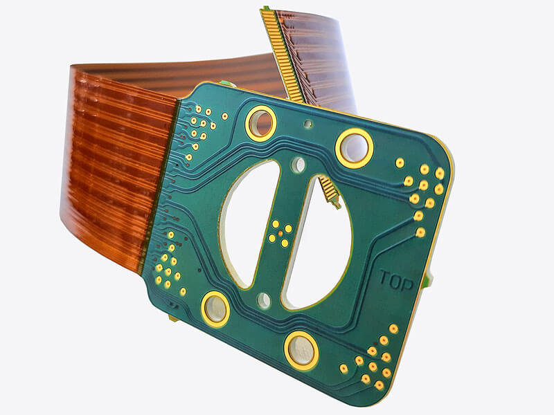
Rigid-flex and semi-flex
Rigid-flex PCB are used when the PCB in the operation is exposed mechanical movement or vibrations, also if spatial conditions do not allow any other solution.
Becker & Müller is one of the specialized manufacturers of rigid-flex and semi-flex PCB and with this development competence we like to already be available for our customers in the development phase.
High-frequency PCB (HF) are used wherever fast signal flows and thus high transmission frequencies are required. In order to ensure the integrity of the high-frequency signal flows at the highest possible frequency, the permissible parameters must be precisely determined and implemented. We at Becker & Müller are your competent manufacturer and development partner in this regard.
Impedance-controlled PCB are used at high frequencies and steep switching edges to ensure signal integrity. Reflections can cause signals to superimpose, which can lead to errors and unreliability of the entire assembly. Becker & Müller is your specialist for the production of impedance-controlled PCB.
Compared to standard FR4 materials, high-TG materials have a higher temperature resilience. These materials are used wherever the PCB is exposed to particular temperature or current loads and a higher continuous operating temperature is required for the reliability of the PCB.
The accommodation of power electronics and the associated extremely high current intensities require special specifications of the carrier circuit boards. We at Becker & Müller have customized solutions for the production of high-current/thick copper PCB.
Aluminum core PCB – also known as IMS (Insulated Metallic Substrates) – are used for mechanical loads, but primarily for thermal loads. The core of the PCB consists entirely of aluminum and is separated from the conductor pattern by an insulation layer.
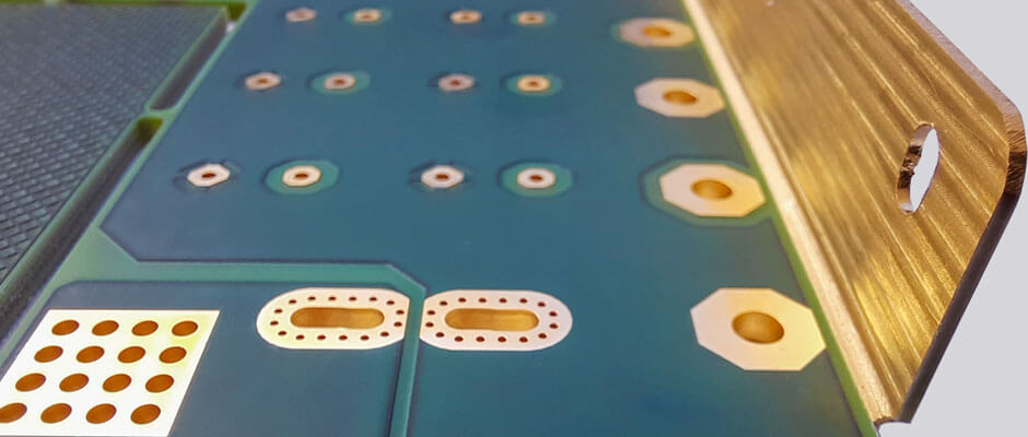
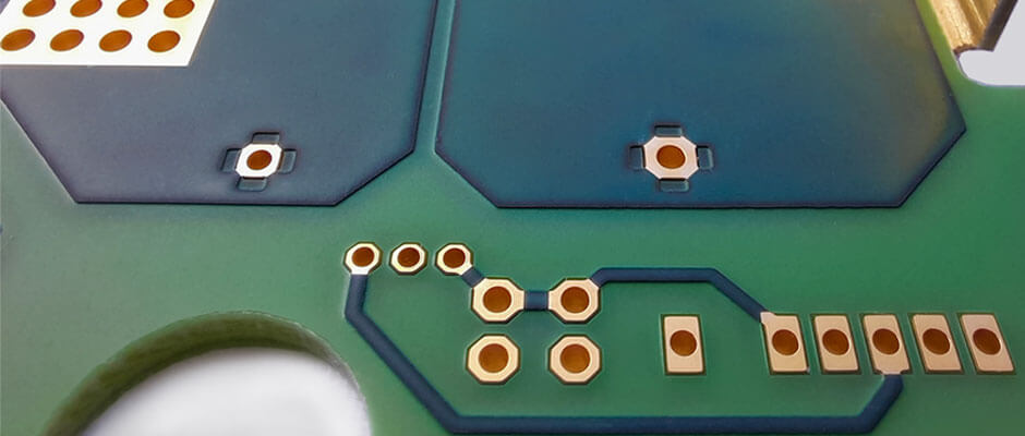
Edge metallization (PTH-contour), special contours, countersinks and depth millings, blind vias, buried vias, plugs, special surfaces or colored solder masks, silk screen, coverlay and bluemask, plugging and more: We at Becker & Müller are the ideal manufacturer and development partner when it comes to very special types of PCB.