Multilayer
circuit boards

Complexity has a name

A multilayer PCB consists of more than two superimposed layers on which traces can be applied and connected by blind- or through-hole plating. Multilayers are especially used, when complexity of the circuits to be implemented on the PCB increases. Depending on structure and layout we at Becker&Müller manufacture PCB with up to 20 layers.
Multilayer Leiterplatte

Manufacturing of multilayer PCB

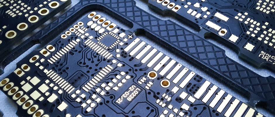
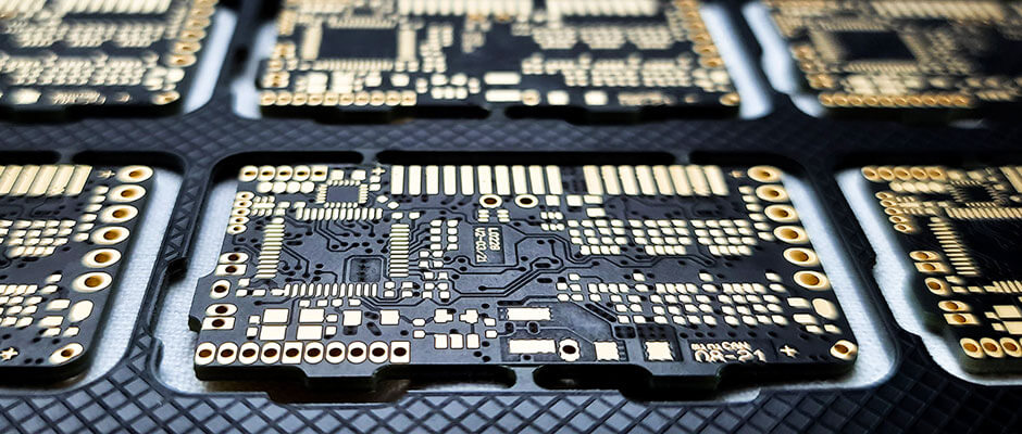
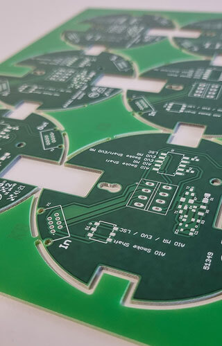
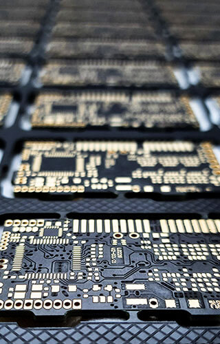
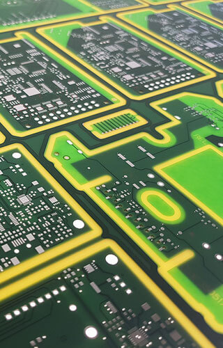
At Becker&Müller we count, with deep expertise and decades of experience, to the top companies when it comes to manufacturing of PCB. Here we want to show you what is important in the production of multilayer PCB. 
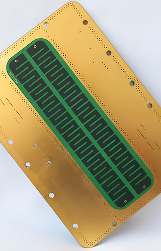
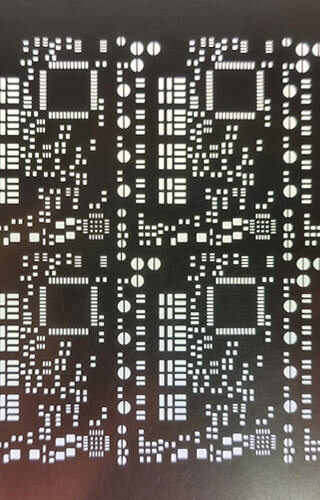
In order to ensure an exact alignment of the inner layers of the multilayer before the pressing process, these are recorded by an optical registration system, automatically aligned to each other, fixed and if necessary riveted. It is similar in the subsequent drilling process, in which any deviations caused by the effects of pressure or temperature during the pressing process must be taken in attention. By using optical measurement of the registration marks applied to the internal cores, the drilling pattern is automatically adjusted to alignment (warping and offset) of the inner layers.
Multilayer PCB

Quality control in multilayer production

Ensuring everything is fitting is one of Becker&Müller‘s basic principles in the manufacturing of printed circuit boards. To guarantee maximum quality and functionality of the multilayers the structure of traces, both the inner layers and the outer layers of the pressed multilayer, is checked by using AOI (Automatic Optical Inspection) and tested by an electrical test (E-Test). Using therefore most modern equipment and trained staff is part of our company philosophy. And that makes us a top manufacturer of all types of PCB!

Multilayer circuit boards

Manufacturing steps

  • phototechnical structuring of the inner layer cores
  • etching the inner layer cores
  • AOI (Automatic Optical Inspection) of the inner layer cores
  • registration and alignment of the inner layer cores (layer count > 4)
  • pressing the multilayer in the multilayer press
  • drilling
  • cleaning of borehole wall
  • direct metallization
  • phototechnical structuring
  • electroplated copper construction
  • etching
  • AOI of outer layers
  • optional solder mask, silkscreen
  • coating of soldering surface
  • electrical test (e-test)
  • contour processing

Materials

  • FR 4 TG 135
  • FR 4 TG 150
  • FR 4 TG 170
  • polyimide
  • PTFE
  • ceramic based material
  • various high-frequency materials
  • more on request
Multilayer Grafik

Specialist for your requirements for 37 years

Ordered. Delivered.
The fastest way to the perfect printed circuit board is via our EXPRESS-SERVICE.