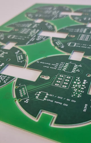
Technology and quality of our circuit boards are among our highest demands. To be constant on to produce at the highest level and also to meet the high technological demands, Becker & Müller has a modern machinery, plant and equipment park. This park is always optimized and kept up-to-date through continuous investments. The same applies of course to the manufacturing processes. Last but not least, it is the joint development together with the customer and their requirements that serve as innovation drivers and reveal optimization potentials.
Quality control
Quality control accompanies the entire manufacturing process of the PCB. Our test standard is the IPC A-600 class 2 – of course, tests according to the acceptance criteria of class 3 are also possible. Even during production, the circuit boards are subjected to various control and through the following measurements or tests, depending on customer requirements:
AOI (Automatic Optical Inspection)
standard
Layer offset control (automatically when registered by CNC machines, manually x-ray examination)
standard for multilayers
E-test (electrical test)
optional
Impedance control
optional
Preparation and evaluation of micrographs
optional
Initial sample inspection
optional
Mechanical tolerance (dimensions of contours as well as position of holes to traces respectively pads)
optional
Our production highlights
The base of quality and precision is – in addition to qualified employees and highly developed processes – our state-of-the-art machinery and plant park. Some highlights of our production are:
LED direct exposure
Computerized multilayer production
Mechanical precision
Pulsplating
LED direct exposure
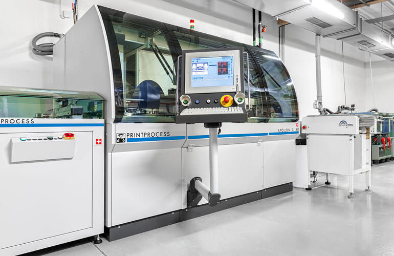
LED direct exposure
In photo technology, we rely on an LED-DI direct exposure unit from Swiss Printprocess AG. Direct exposure has numerous advantages for prototyping. It guarantees a high quality of the PCB thanks to the highest precision and manufacturing accuracy. The capability to expose extremely filigree traces in combination with the automatic alignment of those layouts to the panel respectively its drilling pattern creates its own standards in quality. Because direct exposure does not require any film – beside energy and the use of chemicals – above all, time can be saved and flexibility can be increased. In connection with the industry 4.0 ideas, it is possible for Becker & Müller – thanks to the shortest response time, fast product changes and highest precision – to respond to customer wishes or requirements and nevertheless to guarantee the highest production speed.
Computerized multilayer production
Computerized multilayer production
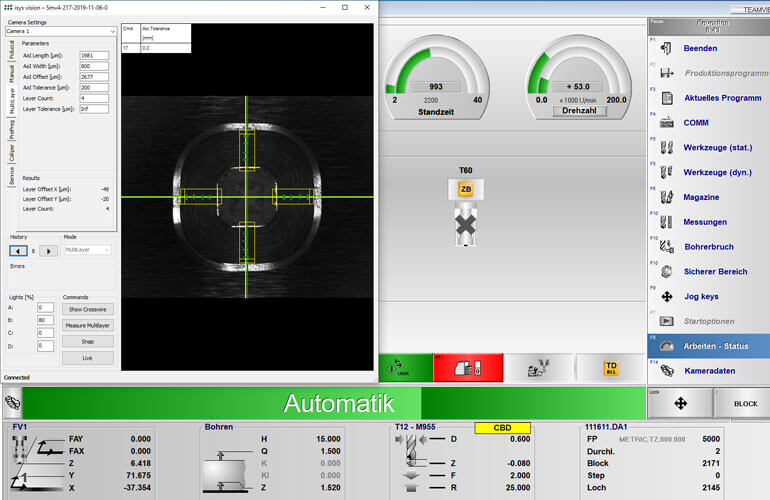
Our multilayer production is supported and supervised by a specially self-programmed software. This determines, using camera registration data, the layer offset or the moving away of the pressed multilayer. Corresponding correction values are then calculated. These are used for compensation in the subsequent drilling and exposure process, in order to optimally adapt the drilling and traces of each panel to their inner layers. Together with an layer offset check – using an x-ray machine – after the drilling process, the occurrence of possible electrical faults on the PCB can be considerably minimized.
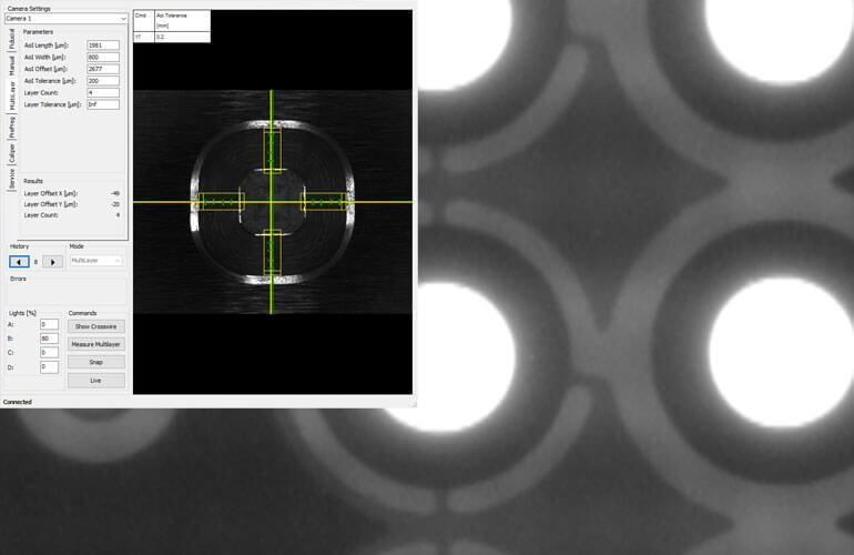
Mechanical precision
Mechanical precision
Our CNC drilling and milling machines are equipped with a camera registration system which detects registration marks on the frame of the panels or on the individual circuit board itself. In this way, the software of the CNC machine compensates for any position deviations respectively fits drillings and millings to the traces or to the connection pads. In connection with process-optimized tool parameters, compliance of mechanical tolerances of < 20 μm (in terms of dimensional accuracy and position accuracy between drilling/milling and traces) is made possible. Using an optical measuring machine – a CNC-video-measuring-microscope – compliance with the required tolerances can be checked and measurements protocols are created.
Pulsplating
Pulsplating
Pulsplating describes a special copper plating process for galvanic copper construction. The aim is to achieve a layer thickness distribution that is as even as possible. This is particularly important for our PCB-Mix (because of the inconsistent copper distribution on the various PCB on one panel) and generally beneficial for holes with a large aspect ratio. With pulsplating, a galvanic rectifier applies a positive followed by a temporal shorter but significantly higher negative DC voltage to the PCB panel. This makes the copper areas, which have a high current density, passive and consequently less copper is built on.
Production Highlights
The base of quality and precision – besides skilled employees and smart processes – is our ultramodern machine and plant park.
LED direct exposure
In photo technology, we rely on an LED-DI direct exposure unit from Swiss Printprocess AG. Direct exposure has numerous advantages for prototyping. It guarantees a high quality of the PCB thanks to the highest precision and manufacturing accuracy. The capability to expose extremely filigree traces in combination with the automatic alignment of those layouts to the panel respectively its drilling pattern creates its own standards in quality.
Because direct exposure does not require any film – beside energy and the use of chemicals – above all, time can be saved and flexibility can be increased. In connection with the industry 4.0 ideas, it is possible for Becker & Müller – thanks to the shortest response time, fast product changes and highest precision – to respond to customer wishes/requirements and nevertheless to guarantee the highest production speed.
Computerized multilayer production
Our multilayer production is supported and supervised by a specially self-programmed software. This determines, using camera registration data, the layer offset or the moving away of the pressed multilayer. Corresponding correction values are then calculated. These are used for compensation in the subsequent drilling and exposure process, in order to optimally adapt the drilling and traces of each panel to their inner layers. Together with an layer offset check – using an x-ray machine – after the drilling process, the occurrence of possible electrical faults on the PCB can be considerably minimized.
Mechanical precision
Our CNC drilling and milling machines have camera registration systems which detect registration marks on the frame of the panels or on the individual circuit board itself. In this way, the software of the CNC machines compensates for any position deviations respectively fits drillings and millings to the traces or to the connection pads.
In connection with process-optimized tool parameters, compliance of mechanical tolerances of < 20 μm (in terms of dimensional accuracy and position accuracy between drilling/milling and traces) is made possible.
Using an optical measuring machine – a video measuring microscope – compliance with the required tolerances can be checked and measurements protocols are created.
Pulsplating
Pulsplating describes a special copper plating process for galvanic copper construction. The aim is to achieve a layer thickness distribution that is as even as possible. This is particularly important for our PCB-Mix (because of the inconsistent copper distribution on the various PCB on one panel) and generally beneficial for holes with a large aspect ratio.
With pulsplating, a galvanic rectifier applies a positive followed by a temporal shorter but significantly higher negative DC voltage to the PCB panel. This makes the copper areas, which have a high current density, passive and consequently less copper is built on.
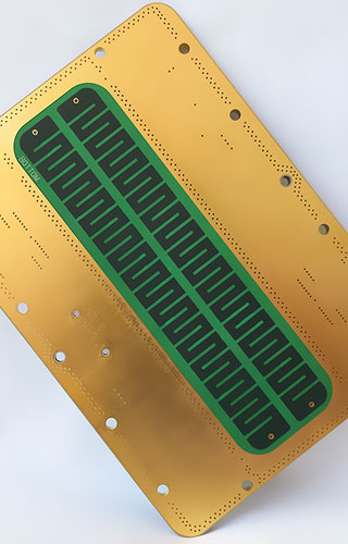
Ses line
Etching is one of the most important process steps in PCB manufacturing – and together with the exposure at the same time one of the most demanding. In prototyping it depends alongside precision primarily on flexibility and speed. For this reason for structuring of inner and outer layers we rely on the combination of LDI and SES line (Stripping – Etching – Stripping).
This 15 meters long system was designed specifically for our needs, it consists of three main modules and uses a patented vacuum etching system. Differences in the etching result between the top and bottom sides of the PCB panels are reduced to a minimum. A special nozzle arrangement enables the increase of spray pressures and throughput speed a plus for precision and output. Process reliability is achieved through permanent monitoring of the medi- ums in combination with automated (re-)dosing. Environmental protection is also not neglected: by using an additional cascade, the system goes beyond legal regulations and reduces the amount of flushing water by a full 50%.
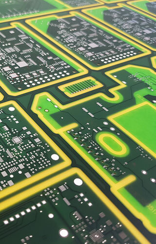
Impedance control
To ensure signal integrity in applications with high frequencies and steep switching flanks, a prior calculation and subsequent control of the conductor impedance is recommended. With us, you can rely on an experienced spe- cialist in the production of impedance-controlled PCB. In order to counteract unwanted capacitive effects, desired parameters – such as conductor dimension, layer stack or base material – are controlled by means of a special software of the market leader Polar Instruments GmbH. If necessary we adjust this parameters on the PCB to reach the desired result.
This means: these parameters are manageable in PCB production. Due to the high process reliability of our production, compliance with the industry standard impedance tolerance of ± 10% can be guaranteed. A final impedance control by means of a representative test coupon ultimately delivers the exact value. The predetermined target impedance is compared with the measured actual value and recorded in a test report.
Certifications
Guidelines
Manufacturing guideline IPC A-600 (acceptance criteria for PCB)