Specials

Electric

Edge metallization (PTH-contour)

In addition to through-hole plating respectively metallization of bores, it is also possible to metallize and coat edges as well as depth millings and countersinks with the desired surface finish.

Mechanically

Special contours

Special contours are available for all types of PCB. Depending on the thickness, the circuit board can be milled inside with a minimal tool diameter of 0.5 mm. Also, edge metallization and coating are possible. By special arrangement special tool geometries can also be used.

Countersinks and depth millings

By choosing different tools countersink holes can be manufactured with different angles, grooves can be also manufactured with angled edges down inside. Metallization and coating is also possible for countersink holes and depth millings.

Blind vias and buried vias

Blind vias and buried vias are used for design optimization of the PCB layout. A bling via is a plated-through hole between the outer and one or more inner layers. A buried via, on the other hand, denotes the plated-through hole between two or more inner layers. The advantage of both via types is the increase of packing density of the circuit board and the associated reduction in dimensions. Please note our design-rules.
Grafik Buried und Blind Via

Plugs (gold, bevel)

Plugs respectively all surfaces that are subject to particular wear can be coated with special plug gold. This hard gold is electroplated applied and is particularly resistant to mechanical abrasion. In order to make it easier to insert the plug, it is also recommended to bevel the plug on both sides.

Mechanical precision

Mechanical accuracy becomes more and more important in manufacturing of circuit boards. By combining high-precision CNC machines with the most modern photo technology – LED direct exposure – we can already manufacture a position accuracy between the holes and traces of < 20 μm. A special measuring machine – a video measuring microscope – is used to ensure compliance, a measurement report is created.

Surface

Surface finish

Released connection areas on the PCB are coated with a final surface finish after application of the solder mask. This coating protects against oxidation of the otherwise exposed copper and thus increases the shelf-life duration of the finished circuit board. Another advantage is the favoring of the later soldering process. The following surface finishes can be selected for the coating:
  • HAL lead-free (Hot Air Leveling)
  • chemically SN
  • chem. Ag
  • chem. Ni/Au (ENIG – Electroless Nickel Immersion Gold)
  • chem. Ni/Pd/Au (ENEPIG – Electroless Nickel Electroless Palladium Immersion Gold)
  • chem. Pd/Au (EPIG – Electroless Palladium Immersion Gold)
  • galvanic Ni/Au (hard gold)
  • galv. Au (fine gold)
  • Entek (OSP – Organic Solderability Preservative)
The surface finish is to be selected depending on the area of application and requirements. We are happy to advise you on the selection.

Colored solder masks

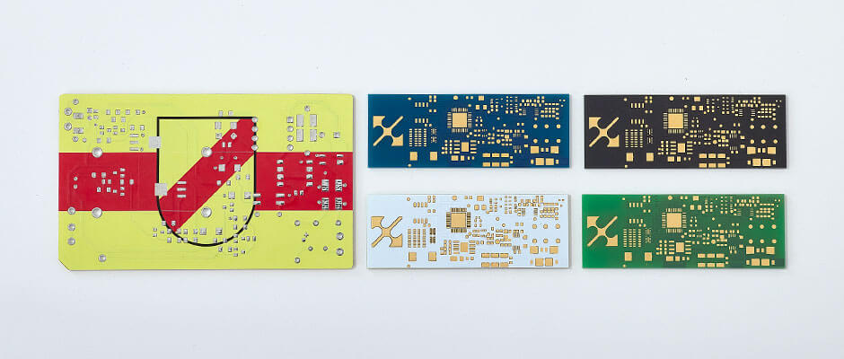
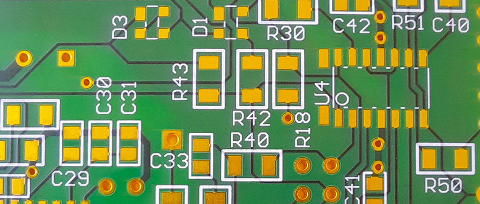
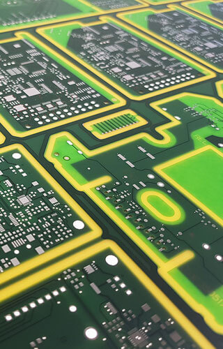
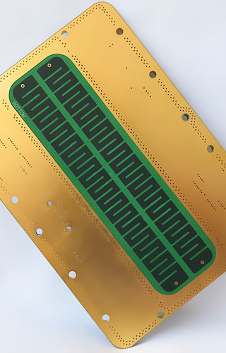
In addition to the standard colors green, white and black, solder masks are on request also available in other colors such as blue, yellow and red.

Silk screen

Silk screen, respectively assembly printing, can be applied in the standard colors white and black. Other colors are also possible on request.

Coverlay on PCB surface

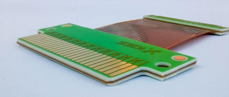
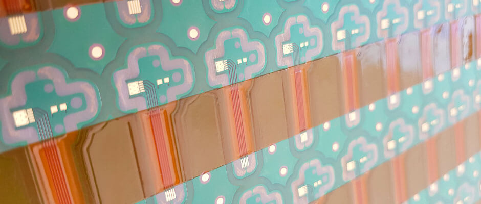
As an alternative or in addition to the solder mask, the surface of the circuit board can be covered and so protected by a coverlay, respectively a cover foil. These special masking films are resistant to abrasion and exhibit dielectric strength and therefore, according to IPC – in contrast to solder mask – to be used as an insulator.

Bluemask (peelable mask)

On request, selected areas of the circuit board can be covered with a special peelable mask – a so-called bluemask. These areas are protected during the soldering process, after that the bluemask can be easily removed without leaving any residue. The aim is to enable a temporally staggered soldering of different areas of the PCB.

Plugging

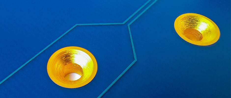
In the plugging process, vias are sealed with a dielectric. Optional the surface of the filled hole can also be metallized. Plugging can be used with conventional vias as well as with buried vias. The advantage lies in the design optimization of the circuit board layout by the possibility of using the sealed holes as a solder pad or as a landing pad for blind vias.

Others

Extensive base materials

To be able to meet our demand for the promised fast delivery times we have an extensive stock of base materials. Next to common standard materials also various exotic base materials of different dimensions and thicknesses are available directly from stick. An excerpt of the most common materials is:
  • FR4
  • High-TG
  • CEM1
  • Rogers
  • PTFE
  • Polyimide
  • IMS (aluminium core)
Other base material types are also available on request. We are happy to advise you in selection of suitable materials for your application.

Copper foils

In addition to our extensive range of base materials, our material storage also contains different types of copper foils. The following thicknesses are available from stock: 9/12/18/35/70/105/200/400μm. More copper foils are available on request.

Hybrids made from different base materials

Multilayers can also be manufactured as hybrids made from different base materials. Our extensive base material store benefits us in this.

PCB thickness up to 8 mm

Our production machinery enables to produce circuit boards with a thickness of up to 8 mm in the standard process. Multilayers made of pure PTFE are so possible up to a thickness of 6 mm. In addition to standard production, it is of course, in coordination with the customer, also possible to achieve even more extreme thicknesses.

Connection of PCB with ceramic block

To enable an improved head dissipation, we have developed – as an alternative to metallic heat sinks – a process that enables us to connect the circuit boards to solid ceramic blocks. For more information, please contact us.

Connection of PCB with heat sinks

In order to enable an improved heat dissipation, it is possible to connect the PCB to an external heat sink. Depending on requirements and surroundings the connection can be produced by gluing or – analogous to multilayer production – by pressing. As an alternative to common metal heat sinks, we have developed a process which enables us to connect the PCB to solid ceramic blocks. For more information, please contact us.

Quality assurance and documentation

Quality is our top priority! Our company is certified according to quality management standard DIN EN ISO 9001:2015. In addition, our circuit boards go through a wide variety of measurement and testing procedures which enable us to control and guarantee the quality standards. Documenting our quality is equally important. In addition to e-test protocols, initial sample test reports and impedance control reports, further customer-specific measurement and test reports can also be created. Micrographs of individual circuit boards can also be made and evaluated.

Specialist for your requirements for 37 years