High-performance high-frequency systems in standard printed circuit board technology using clever signal lines
As the result of a BMWK-funded joint project with the Technical University of Berlin, Becker & Müller is presenting a technology that makes it possible to manufacture entire high-frequency systems extremely cost-effectively with low signal losses. For this purpose, miniaturized waveguide structures are manufactured using conventional PCB technology. Based on this concept, it was possible to build and measure extremely low-loss structures up to ≤ 140 GHz, with the system concept enabling much higher frequencies. In addition to simple point-to-point lines, branches with adjustable pitch ratios, filter structures and antennas for radiation along the surface of the PCB and perpendicular to it were developed. All line sections are designed in such a way that a user can freely configure his target system from the individual blocks on the PCB. Becker & Müller thus underlines its reputation as a manufacturer and partner for sophisticated PCB solutions away from mass-produced products.
Higher frequencies as a requirement
Current and future communication systems such as 5G, 6G and radar sensor technology are operating at ever higher frequencies in order to take advantage of the resulting benefits in data rate or measurement accuracy. However, the availability of corresponding high-frequency transmitter and receiver chips is only one side of the coin. The individual electronic components must ultimately be assembled into a complete system. This is where the established PCB technology, the previous favorite, comes under pressure in terms of the cost-benefit ratio: “Due to the so-called skin effect, the high frequency components are primarily conducted on the surface of the conductor tracks,” explains Janik Becker, Managing Director of Becker & Müller Schaltungsdruck GmbH. “There, however, the signals see a lot of the PCB material, which significantly absorbs power. Even the use of more expensive high-frequency PCB materials and an electromagnetic design with shielding conductors only help to limit the signal absorption caused by the base material to a limited extent. This means that current PCB technology can only be used meaningfully up to about 60 GHz.”
How can this now be resolved? This question was the focus of a federally funded joint project called “Tera-Hertz PCB: Development of Design Guidelines and Manufacturing Processes for the Integration of Terahertz Systems into Standard Printed Circuit Boards.” The project partners were, on the one hand, the renowned Technical University of Berlin and, on the other hand, the PCB expert Becker & Müller: As a medium-sized family-owned company based in Steinach in the Kinzigtal region of southern Germany, Becker & Müller is regarded throughout Europe as one of the most accomplished experts for special, sophisticated solutions in the field of PCB manufacturing.
The core premise of the project was the use of existing production machinery in PCB manufacturing in conjunction with the search for a cost-optimized solution. “The basic idea of the solution concept was to create waveguides in the PCBs by milling processes, to galvanically metallize the waveguides and to close the structure with a metal plate, e.g. in the course of SMD assembly,” explains Janik Becker. “In this way, a closed waveguide is formed, whereby the signal conducted inside no longer interacts at all with the PCB material, which is after all beyond the metal barrier. This means that we can use the comparatively cheapest FR4 material here – even for very high frequencies far beyond 100 GHz.”
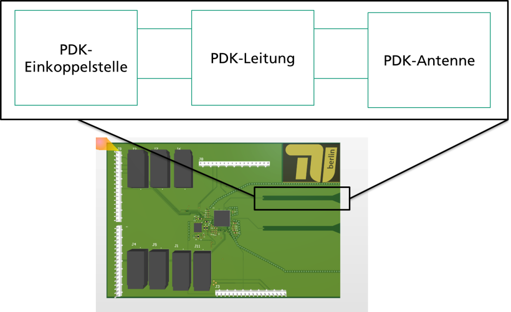
Furthermore, this technology offers the possibility of integrating antennas directly: Firstly, as funnel-shaped extensions of the waveguide in the sense of a horn antenna at the edge of the PCB for lateral radiation, and secondly, as a slot antenna through recesses in the cover plate for radiation perpendicular to the PCB surface or at an angle defined by the slot spacing. The modular system developed in this way is supplemented by waveguide structures that split the signal into different channels in a defined power ratio, filter structures, coupling points to classic conductor tracks on the PCB surface and bent conductor tracks. “These elements were prepared in a modular fashion for the PCB design, so that the customer can simply assemble and have his high-frequency system manufactured by drag & drop – an enormous gain in simplicity, convenience and individuality,” Becker is pleased to say.
Higher frequencies as a requirement
In development, it was important to remain compatible with standard PCB processes at all times in order to be able to integrate the new type of PCB-integrated waveguide technology cost-effectively into new systems. First, a PCB is manufactured as usual with all the required inner layers. In the next step, the waveguide structure is milled into the PCB material. The dimensions of the waveguides depend on the frequencies to be conducted, e.g. for 60 GHz 2.8 mm wide and 0.8 mm deep. The walls of the cavities created in this way are then electroplated with Cu (approx. 30 µm). To close the waveguide, we solder a suitably cut 70 µm copper cover sheet, here laser cut, to the edges of the trenches. This assembly with the sheets can be done, for example, in the SMD assembly step as well.
Based on this technique, the following functional blocks were realized:
- Line sections
- Coupling and decoupling structures to (coplanar) striplines on the PCB surface
- Horn antennas with radiation characteristics starting from the sides of the PCB
- Slot antennas for radiation perpendicular to the PCB surface (or tilted at a defined angle to it)
- Branches with defined division ratio of the signal strength
- Frequency filter structures
Findings from the research project:
Comparison with conventional line structures
In RF technology, microstrip or ground coplanar lines are typically used. These have the advantage that they can be used to transport power even at direct current. On the other hand, these lines have additional losses at higher frequencies due to the substrate material, but also at the same time due to roughness at the various interfaces between metal and substrate. To solve these challenges, such lines can also be implemented in waveguide form and, as described, integrated directly into PCB technology. However, the waveguides have the disadvantage that they do not have classical TEM modes, but either a TE or TM mode. This makes the cutoff frequency directly dependent on the dimensions of the waveguide (only with TEM modes is there a line at DC). Therefore, when comparing both types of lines, the picture is that the classical line types show better performance up to about 50 GHz than the demonstrated waveguide. The reason is, as described, that the cutoff frequency is at about 60 GHz. After that, the losses remain relatively stable over the waveguide, with the losses dropping further for the conventional line.
Within the research project, other structures were investigated in addition to the transmission lines. The details of these are presented in the next section.
Components and their performance characteristics
Within the project, various subcomponents were investigated. The focus was on preparing these subsystems within the project in such a way that they can later be used to build up arbitrary systems like building blocks. The line as well as the antennas, filters and power divider structures (signal/power split) were designed and electrically characterized in detail. It is shown that the structures are significantly more powerful than comparable structures in planar technology. These structures were then transferred to a database, which is called PDK. PDK stands for physical designer kits.
Application of the PDKs
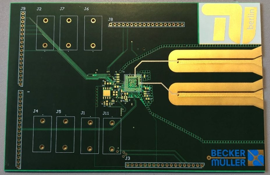
After the PDKs were derived, a demonstrator system could be assembled based on them. This is a 79-GHz short-range radar. Structures were then selected from the existing PDKs, which were assembled in layout for the demonstrator.
Typically, a schematic is designed for such a circuit. In the schematic, the PDK models were directly integrated, so that the structures can be placed directly in the layout. The final layout with the PDK structure is shown in the following graphic.
Design rules are then used to check that lines or distances are as large as necessary but as small as possible. Based on this information, the critical RF lines and power supply are placed first and then the remaining components are placed. The final design is shown in the figure below.
Discussion points
The work has shown that it is possible to incorporate waveguide structures into printed circuit boards using established PCB technology. This can be incorporated into the production process in such a way that further assembly of the PCB is possible as usual. Measurements have confirmed that for applications with frequencies above 60 GHz, the waveguide structures have significantly lower losses – a factor of 2. For simple adaptation of the technology to new applications, building blocks have been defined from the basic structure of a high-frequency system, which make it possible to assemble such systems – without simulations of the high-frequency properties – and to supply the necessary production data for this at the same time. These PDKs were successfully integrated into the development process, see Figure 7.
Partner for the design of high-frequency systems
Becker & Müller CEO Janik Becker is more than satisfied with the findings: “The cooperation with our partners from the TU Berlin was a great experience – both technologically and personally. After the successful completion of the project, it is now possible for us at Becker & Müller to provide support in the design of high-frequency systems by using the PDKs.” In view of the derivation of internal design rules to the respective blocks as well as their validation, both function and feasibility of the waveguide structures are thereby given. “The first projects for practical implementation are already in the planning stage,” says Becker. “We look forward to receiving further inquiries, which our team will handle personally, competently and very quickly as usual.