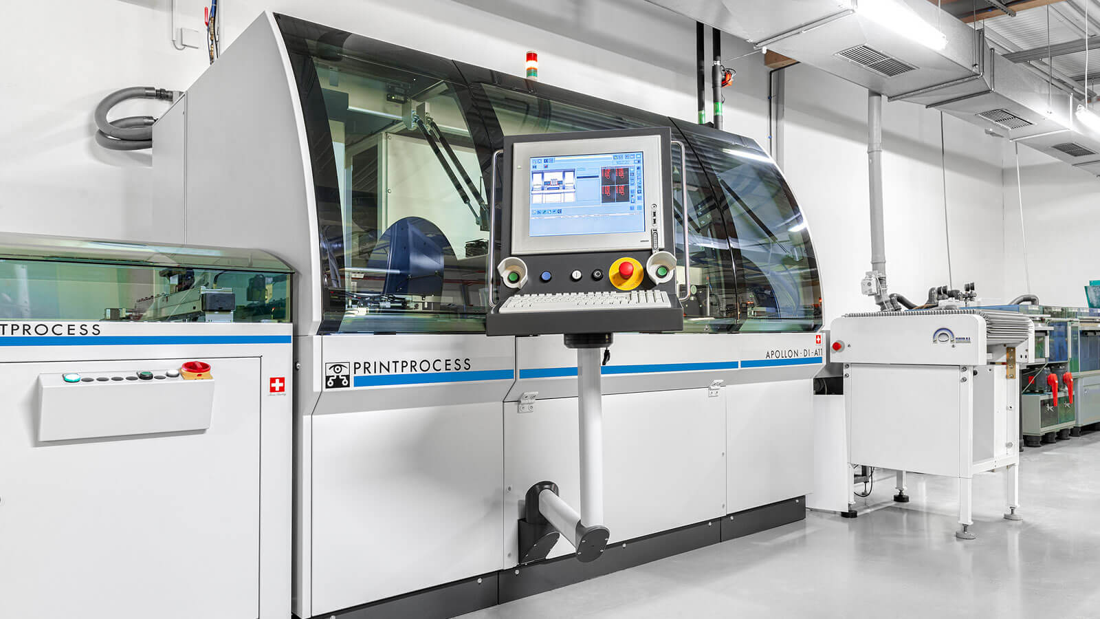
“From a technological point of view, the exposure of printed circuit boards is a challenge the further you penetrate into very small structures,” explains Janik Becker. The 30-year-old industrial engineer joined the company in the middle of last year and is now the third generation to lead the family business into the future. He is supported by a strong team of specialists, as well as by Xaver Mueller, who, as a co-founder, has handed over his responsibilities to Becker jr., but continues to contribute his deep experience and expertise. “The purchase of our automated maskless exposure system nine years ago was a real quantum leap in PCB production at Becker & Mueller. Up to now, the limiting factors have been upstream and downstream processes, after these had also been modified, the exposure had to be brought up to date. With the optimization of the system, we have again taken a huge step forward.”
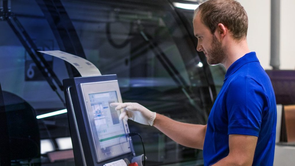
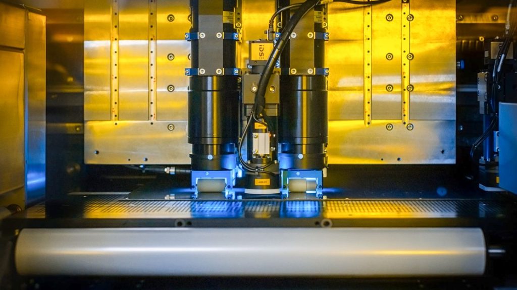
The exposure from the Swiss manufacturer Printprocess AG, aptly named “Apollon” after the god of light, can be used multifunctionally. In addition to the photo-technical structuring of the PCB layout and solder mask, an automatic thickness measurement of the PCB panels is integrated. Because in order to achieve optimal exposure, it is important – as with a photo camera – to set the focus correctly. Previously, this was done using a manual measurement by the operator and an entry in the imagesetter’s job file. The newly optimized system now implements this process fully automatically using an internal measuring unit that independently sets the focus during the exposure process and thus ensures a highly precise adaptation to the circuit boards surface: “For our customers, this is a plus in terms of safety and quality” says Becker.
In addition, the optical exposure unit was exchanged. This allows a much higher resolution to be achieved, which protects the LED light source and allows a slightly shorter exposure time for solder resists. Thanks to the higher resolution, even more filigree structures in the range of up to 75 µm can now be imaged: “For us and our customers, these are advantages on many levels.”
The ability to penetrate into such microscopically small structures not only offers optimization potential for existing solutions, but also opens up new fields of application, as Janik Becker confirms: “In many future-oriented industries, miniaturization is an important key issue. With our improved possibilities of PCB exposure we have our finger on the pulse.” More precise, more efficient, better: the consistent technological optimization of the processes underscores Becker & Mueller’s reputation as an absolute specialist in the manufacture of sophisticated PCB.