High current and thermal management are driving the advancement of modern PCB technology.
PCB designers are often confronted with the problem that separate PCB have to be used for the different functional areas of an electronic device. Because of the different thermal loads on the materials, the control and power sections often cannot be implemented on a single circuit board. Becker & Müller offers a process with which these two areas can be integrated on a single PCB – the copper-inlay-technology.
Copper is usually processed on or in printed circuit boards with a thickness of up to 105 μm. The heat generated during operation can often only be effectively dissipated from the circuit board by means of large-volume heat sinks. In order to prevent thermo-mechanical deformations, the PCB in the housing often have to be mounted with stable brackets and heat dissipation elements.
With copper-inlay-technology, metal cores with thicknesses of up to 1,000 μm are laminated into or on a PCB with at least two conductor levels. These thermally conductive and mechanically reinforcing metal inlays (e.g. made of copper) can be used as high-current conductors in certain sections. So they complement the electrical layout and at the same time serve the purpose of heat management by dissipating the heat that is generated. Electrical and thermal properties of the insert material are used simultaneously.
As a specialist in the field of prototyping, Becker & Müller decided to use copper as the material for the inlays after various tests and investigations of the inlay technology. In addition to the test results, the well-known properties of copper and the possibility of integrating the method into existing processes were decisive for the choice of the inlay material. In addition, most applications and market requirements can be covered with it. In special cases, in addition to copper, there is the cheaper option of using aluminum for heat dissipation, but if electrical properties are also important, copper remains the material of choice. Alternatively, especially for high-current applications, Wirelaid technology would be conceivable, for example.
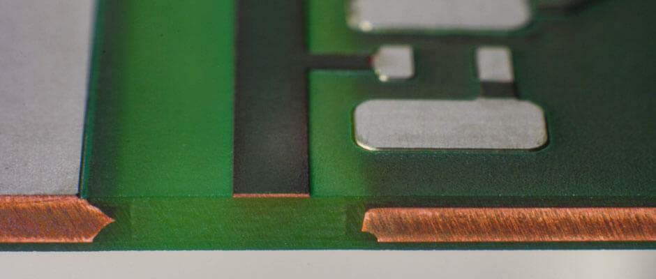
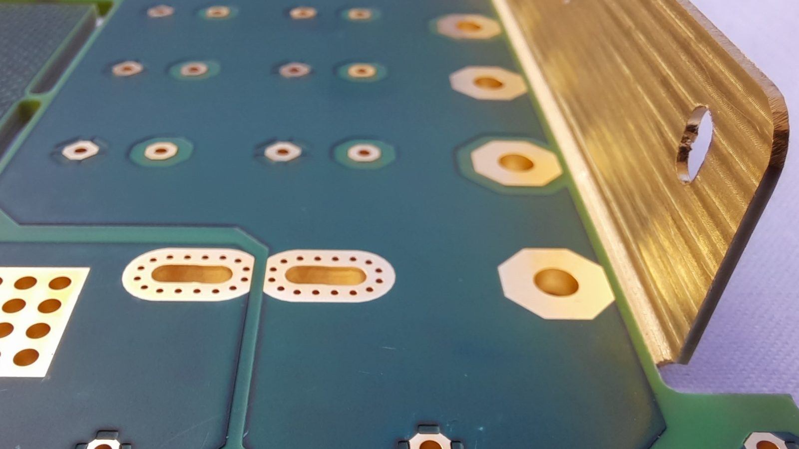
The copper inlays can be placed in intermediate layers of multilayers or placed directly on the circuit board surface in suitably milled indentations. Inlays, which are designed on the surface of the PCB, offer the possibility of mounting or soldering the components directly on it. Depending on the design, no – or at least less – additional heat dissipation through separate cooling elements, special housing design or other complex precautions is required.
Production using copper-inlay-technology may be more complex than with conventional circuit boards. The technology requires additional work steps and not every step can be automated. The inlays have to be processed separately and prepared for the production process. For example, they go through a drilling and milling process as well as a surface treatment before use. Although these processes are part of the standardized production processes, they are additional. The carrier material (mainly FR4) is precisely milled and the inlays are then inserted into the recess by hand. A relatively high proportion of manual work is required here. Machine insertion is not an option as it is not cost-effective to implement such a system for smaller batches.
Due to the specifications and the tolerances that occur in the manual insertion process, there is a gap between the base material and the inlay. This is necessary for assembly and is then reliably filled with resin. Other filling materials were originally experimented with, but maintaining the tightest tolerances allows the use of standard processes and materials. However, the laminating process of the inlays turned out to be challenging, but it is now also standardized. However, removing excess resin from the inlays still requires an extra production step.
The use of foils with a temperature coefficient of less than 5 ppm/°C for lamination was rejected again. If you want to stabilize a multilayer with the help of such a foil, for example, to a temperature coefficient of 6.5 ppm/°C, which roughly corresponds to the coefficient of ceramic material, then 40 – 60% of the circuit board thickness would have to consist of such foils, otherwise the resin material with its Temperature coefficient of 16 ppm/°C predominates.
At Becker & Müller, a proprietary measurement methodology was developed specifically to test the thermal expansion of the finished circuit boards. The expansion of the finished panel can be measured with the aid of a measuring mask developed in-house. The thermal expansion of the stabilizing material should be as small as possible. The material should be easy to process in a multilayer and then easy to edit. At best, standard material should be used. For the new technology, Becker & Müller prefers FR4 (easy to process) and copper (high thermal conductivity) – those materials that are already established in the manufacturing processes.
When designing the circuit board, copper-inlay-technology now enables the power (with high currents and large structures) and control section (with low currents and filigree structures) to be implemented on a single circuit board – without mutual interference. This means savings in material, size and components. A high-current PCB can contain additional signaling elements and mechanical connections using cables, plug-in contacts or the like can be omitted. This cost saving is combined with the desired property of heat dissipation for the high-current range. Such applications are increasingly in demand from customers. PCB with integrated power supplies that have to carry high currents – currents of up to 800 or 1,000 amperes are possible. This is preferably implemented with copper inlays with a thickness of 1,000 μm, even up to approx. 4,000 μm thickness are possible.
The production of the individual circuit boards with the new inlay technology is more complex and therefore more expensive, but this ultimately means significant cost savings for the later end product. Significantly fewer, smaller and more compact PCB can be used to develop new products, and cooling elements and mechanical connections are no longer required. In addition, molds can be precisely adapted to customer requirements. If the product designer so desires, the copper protruding from the sides of the PCB can be milled away during the final cut, but it can also be used to dissipate heat to the ambient air. This milling contour, including the depth milling steps, is programmed separately at Becker & Müller, so special contour requests from the designers can be easily implemented.
In the DFM-process (Design for Manufacturing), coordination with the customer is carried out in advance and details are discussed (“Where are the limits of what is feasible?”). Data reviews and layout checks are carried out and the results are incorporated into the design of the circuit board. Direct and personal exchange with the designers is important to the Becker & Müller team at DFM. Layouts are thus optimized for the production of the PCB – this benefits the end product and thus the customer.
At Becker & Müller, drive technology, power supply and power supply units were the driving forces behind the introduction of copper-inlay-technology. More and more applications are being added today. For example, in e-mobility, in converters for solar and wind power plants and in power electronics in general, PCB have to transport large currents and temperatures. The higher the power, the more interesting the copper-inlay-technique becomes.
For circuit board production, this means high – and in the future increasing – demands on design and materials. The managing directors Michael Becker and Xaver Müller like to take on such challenges and thus live up to their own claim of always being up to date with the technical possibilities of Becker & Müller.