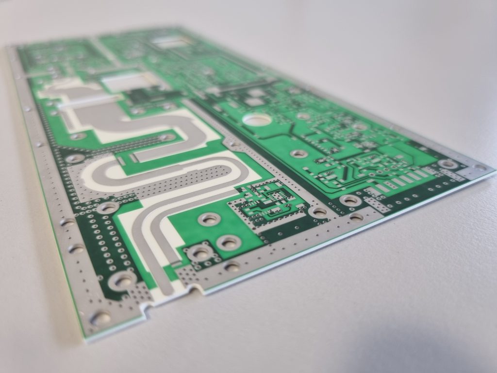
In modern electronics production, PCBs have long since ceased to be seen as pure component carriers, but have established their status as complex, independent components. High-frequency and impedance-controlled circuit boards are gaining in importance.
The electronics industry is developing rapidly – for suppliers this means that they must consistently face the fast development cycles in the industry. Keeping your finger on the pulse of the times is nothing new for Becker & Mueller, as future orientation has always been of great importance to the prototype manufacturer. A challenge that is increasingly in demand – the production of high-frequency or impedance-controlled circuit boards – therefore fits perfectly into the companys portfolio. The devices on the electronics market are becoming smaller, faster and more powerful. In order to be able to meet these requirements, the focus is increasingly on the circuit board itself, away from the purely component-related level. Impedance-controlled circuit boards make clean transmission of high-frequency signals between the components possible in the first place.
Like each component, the PCB is also subject to manufacturing tolerances. These have a significant influence on the functionality and durability of the assembled product. The circuit board must also have certain electrical quality criteria and functional properties. This is the only way to build solid and safe electronic devices. Electronics developers and application engineers from component manufacturers work hand in hand to master the new challenges in terms of miniaturization and increasing operating frequencies.
Problem of high-frequency signals
Increasing frequencies inevitably lead to increasing mutual interference between the signals. Conductor paths running in parallel act like capacitances, whose reactances decrease inversely with the signal frequency. In addition, the longer the lines run in parallel, the greater the capacitance. On the other hand, the inductance increases with ever narrower traces. The higher the capacitance and impedance, the lower the cut-off frequency. This means that the attenuation of high frequencies increases more and more. The resulting low-pass filter turns a clean square-wave signal into a more or less smooth signal. In extreme cases, only the fundamental sine wave remains. Any signal can be broken down into individual sine and cosine oscillations using Fourier synthesis. The amplitudes and phase shifts vary depending on the signal. If these individual oscillations are rejoined at the end of the transmission path, the original signal should be produced again. However, if some of the oscillations are missing due to the low-pass behavior of the transmission path, or if their amplitudes or phase angles are changed, deviations from the original signal result. How large such a deviation may be depends on many factors. On the one hand, the signal input of the integrated circuit must of course process the received signal as if the original signal were present, on the other hand, two signals generated at the same time must also arrive at different inputs at the same time (keyword transit time). The information that is to be processed by the respective system is ultimately contained in the signal form and the chronological sequence of the signals. The manufacturer or developer is responsible for correct signal transmission within the integrated circuit. In his data sheet, he defines the specifications with which this component must be operated in order to avoid malfunctions. The electronics developer who interconnects many of these components must now ensure that the signal path – in other words, what happens to the signal between the components – is within the required specification. So that, for example, a circuit can output the duration of an input pulse correctly at its output, correspondingly steep edges are necessary at its input. Assuming the previous function stage delivers an absolutely clean square-wave pulse, but the transmission path dampens the high signal components too much, then the rising edge of the signal is clearer, which results in delayed switching of the input stage. This already results in a time offset between the two signals. In addition to the attenuation and thus deformation of signals, there is another phenomenon that occurs at high signal frequencies: reflection. It always occurs when the signal propagation time on the line is longer than the pulse duration. Signal distortions can also occur in the case of reflections. A signal line was viewed as a parallel connection of many tiny capacitors and a series connection of many tiny inductances and resistors. For the sake of simplicity, we only consider the capacities here. In reality it is a bit more complicated. The pulse travels from capacitor to capacitor – the following capacitor is charged while the previous one is be discharged. When this pulse arrives at the end of the line, the last capacitor wants to discharge and thereby transfer its charges to the next capacitor. The decisive factor is what is at the end of the line – in extreme cases, for example, nothing. The line is open. However, this also means that there is no next capacitor. The last capacitor is charged, but the previous one is discharged. The whole thing is reversed and the last capacitor gives up its charges to its predecessor. And so the impulse travels back, it is reflected. Strong attenuation and reflection can only be prevented with a so-called impedance-controlled conductor track. This is a performance adjustment. For this, the following condition must be met: the output impedance of the pre-stage must be equal to the input impedance of the secondary stage. In addition, the signal path must have the same impedance (= characteristic wave resistance). Written as a formula: ZA = ZL = ZE. If this requirement is met, then the frequency-dependent attenuation and reflections are greatly reduced or, ideally, even eliminated. The properties of the high-frequency signals are retained. In order to do justice to this formula, the 50 Ω technique is usually used. The component manufacturer ensures that the input and output resistances (actually: input and output impedances) are each 50 Ω. In order to meet the condition for matching described above, the trace must also have this characteristic impedance of 50 Ω. However, the characteristic impedance of a conductor track is usually not known, it depends on the geometry (conductor track width, thickness and distance to the ground plane) and the electrical parameters of the material (dielectric constant). These parameters must be combined accordingly so that a trace also has an adapted characteristic impedance.
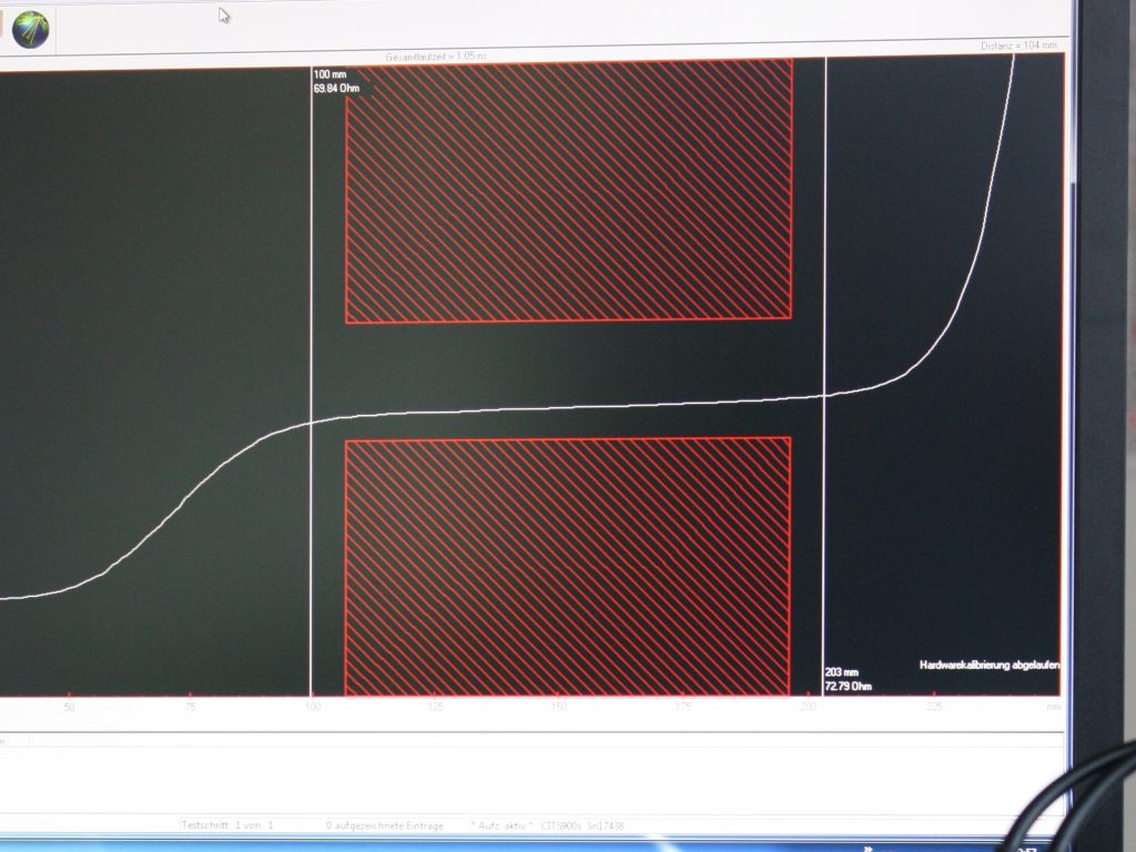
Technological approach of the PCB production
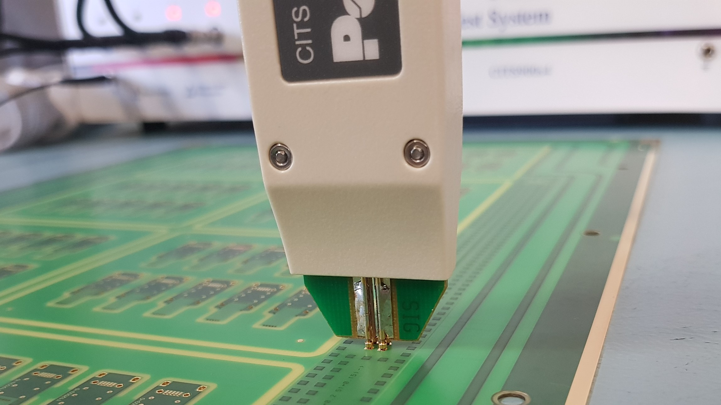
The selection of the base material depends, among other things, on the frequency range. In the event that the properties of simple FR4 are not sufficient for this requirement, the use of special high-frequency materials or substrates is necessary. The HF properties depend on the frequency, these relationships are described in relatively complex physical formulas. Calculation programs help to determine the required values (e.g. the required conductor width can be determined from known values for material constants, circuit board thickness, conductor thickness etc. – this calculation can be found in the service area of our Becker & Mueller homepage). The values determined in this way are then to be adopted as precisely as possible during layout. The circuit board manufacturer is responsible for ensuring that the characteristic impedance of the finished circuit board corresponds to the required value. In order to keep the manufacturing tolerances as low as possible, a great deal of experience and know-how is required. At Becker & Mueller, a special measuring system was set up by the market leader Polar instruments GmbH specifically for the production and testing of impedance-controlled circuit boards. The system determines the actual values of the high-frequency properties exactly, records them and compares them with the required target values and their tolerance.
Development and production – prerequisites for a qualitative result
Ralf Mayr, Managing Director of the company RF Design from Lorsch (Hessen, GER), develops devices for high-frequency technology. They are mostly special solutions for national and international customers. Including well-known ones like ZDF or SES-Astra. The company needs high-quality impedance-controlled circuit boards for its devices. That is why Ralf Mayr has been using the expertise of Becker & Mueller Schaltungsdruck GmbH for a long time. In this way, a trusting and constructive cooperation has developed over the last 20 years. For Mayr, the most important thing is “that the board is not just produced, but that the data is critically examined before production“. If there are any abnormalities or discrepancies when checking the data during work preparation, the experts at Becker & Mueller contact the developers to correct them together. The development of complex high-tech devices can hardly be overseen or controlled by individual processors in the process. Therefore, a trusting cooperation of all specialists involved in the manufacturing process is necessary. In electronics in particular, a very broad and in-depth knowledge of the areas of digital and analog technology, HF and NF technology, signal and power electronics, mechanical and physical material properties and heat management is necessary. RF Design and Becker & Mueller show again and again impressively how a close and cooperative partnership bears fruit.